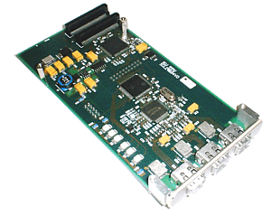
PMC FW2 IEEE1394 Firewire Controller
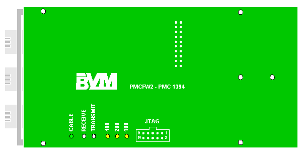
The PMC FW2 is an OHCI compliant IEEE1394 Firewire controller providing three ports via the front panel connectors. This PMC module uses the latest chipset from TI and supports transfer speeds of 100, 200, or 400Mbits/sec. Power is provided to the interface cable to enable the interface (PHY) on remote modules to be powered up enabling loop through operation on powered-off systems. A unique feature of the PMC FW2 is the inclusion of LED indicators on the reverse of the module to assist in the de-bugging phase. These indicators include cable connected, receive and transmit data and speed of operation.
Features
- 32-bit PCI single chip IEEE1394 OHCI controller (Texas TSB12LV26).
- Conforming to IEEE1394-1995 and IEEE1394a-2000 for data rates up to 400Mbits/sec.
- Single chip three port cable transceiver/arbiter PHY (Texas TSB41AB03).
- PHY power is taken from either PCI +12V or cable power enabling a powered down PMC module to forward IEEE1394 data packets.
- Alternate power provider (does not supply power to the cable).
- Configuration EEPROM (1Kbit) for PCI subsystem, subsystem vendor ID and other configuration information.
- Conforms to PMC standard IEEE P1386.1/Draft 2.3 9th October 2000.
- Conforms to PCI Local Bus Specification Revision 2.2.
Applications
- High performance storage interface for industrial PC's or servers.
- Interface to high performance hard disc's.
- Interface to Video equipment for video capture/play-back and editing.
- Interface to document scanners.
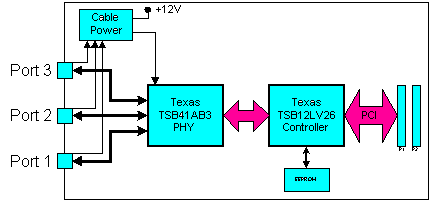
Block Diagram
Board Layout
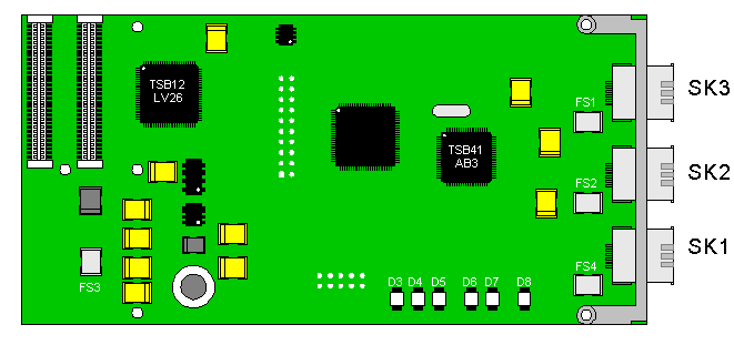
Layout Topside Layout Underside
TSB12LV26 IEEE1394 Controller
The PMCFW2 uses a Texas Instruments TSB12LV26, which is a PCI-to-1394 host controller compatible with the latest PCI Local Bus, PCI Bus Power Management Interface, IEEE1394-1995 and IEEE1394 Open Host Controller Interface Specifications (OHCI). The chip provides the IEEE1394 link function, and is compatible with serial bus data rates of 100 Mbits/sec, 200 Mbits/sec, and 400 Mbits/sec.
As required by the IEEE1394 Open Host Controller Interface (OHCI) and IEEE1394a Specifications, internal control registers are memory mapped and non-prefetchable. The PCI configuration header is accessed through configuration cycles specified by PCI, and provides Plug-and-Play (PnP) compatibility. Furthermore, the TSB12LV26 is compliant with the PCI Bus Power Management Interface Specification, as per the PC99 requirements. The TSB12LV26 supports the D0, D2, and D3 power states.
The TSB12LV26 design provides PCI bus master bursting, and is capable of transferring a cache-line of data at 132Mbytes/s after connection to the memory controller. Since PCI latency can be large, deep FIFO's are provided to buffer IEEE1394 data.
The TSB12LV26 provides physical write posting buffers and a highly tuned physical data path for SBP-2 performance. The TSB12LV26 also provides multiple isochronous contexts, multiple cache-line burst transfers, advanced internal arbitration, and bus holding buffers on the PHY/Link interface.
Major Features of the TSB12LV26s
- 3.3V core logic with universal PCI interfaces compatible with 3.3V and 5V PCI signalling environments.
- Supports serial bus data rates of 100, 200, and 400 Mbits/sec.
- Supports physical write posting of up to three outstanding transactions.
- Serial ROM interface supports 2-wire devices.
- Supports external cycle timer control for customised synchronisation.
- Implements PCI burst transfers and deep FIFO's to tolerate large host latency.
- Provides two general-purpose I/O signals.
- Supports CLKRUN.
TSB41AB3 IEEE1394a-2000 PHY
The PMCFW2 uses a TSB41AB3 PHY, which provides the digital and analogue transceiver functions needed to implement a three-port node in a cable-based IEEE1394 network. Each cable port incorporates two differential line transceivers. The transceivers include circuitry to monitor the line conditions as needed for determining connection status, for initialisation and arbitration, and for packet reception and transmission.
The TSB41LV03 uses a 24.576MHz crystal as a reference - an internal oscillator drives an internal phase-locked loop (PLL) which generates the required 393.216MHz reference signal. This reference signal is internally divided to provide the clock signals used to control transmission of the outbound encoded strobe and data information. A 49.152MHz clock signal, supplied to the associated LLC for synchronisation of the two chips, is used for re-synchronisation of the received data. The power-down (PD) function is disabled on the PMCFW2.
Data bits to be transmitted through the cable ports are received from the LLC on two, four, or eight parallel paths (depending on the requested transmission speed). They are latched internally in the TSB41AB3 in synchronisation with the 49.152MHz system clock. These bits are combined serially, encoded, and transmitted at 98.304, 196.608, or 392.216Mbits/sec (referred to as S100, S200, and S400 speed respectively) as the outbound data-strobe information stream. During transmission, the encoded data information is transmitted differentially on the TPB cable pair(s), and the encoded strobe information is transmitted differentially on the TPA cable pair(s).
During packet reception the TPA and TPB transmitters of the receiving cable port are disabled, and the receivers for that port are enabled. The encoded data information is received on the TPA cable pair, and the encoded strobe information is received on the TPB cable pair. The received data-strobe information is decoded to recover the receive clock signal and the serial data bits. The serial data bits are split into 2, 4 or 8-bit parallel streams (depending upon the indicated receive speed), re-synchronised to the local 49.152MHz system clock and sent to the associated LLC. The received data is also transmitted (repeated) on the other active (connected) cable ports.
Both the TPA and TPB cable interfaces incorporate differential comparators to monitor the line states during initialisation and arbitration. The outputs of these comparators are used by the internal logic to determine the arbitration status. The TPA channel monitors the incoming cable common-mode voltage. The value of this common-mode voltage is used during arbitration to set the speed of the next packet transmission. In addition, the TPB channel monitors the incoming cable common-mode voltage on the TPB pair for the presence of the remotely supplied twisted-pair bias voltage.
The TSB41AB3 provides a 1.86V nominal bias voltage for port termination. The PHY contains three independent TPBIAS circuits. This bias voltage, when seen through a cable by a remote receiver, indicates the presence of an active connection.
The line drivers in the TSB41AB3, operating in a high-impedance current mode, are designed to work with external 112W line-termination resistor networks in order to match the 110W cable impedance. One network is provided at each end of a twisted-pair cable. Each network is composed of a pair of series-connected 56W resistors. The midpoint of the pair of resistors that is directly connected to the twisted-pair A terminals is connected to its corresponding TPBIAS voltage terminal. The midpoint of the pair of resistors that is directly connected to the twisted-pair B terminals is coupled to ground through a parallel R-C network. The values of the external line-termination resistors are designed to meet the standard specifications when connected in parallel with the internal receiver circuits. An external resistor connected between the R0 and R1 terminals sets the driver output current, along with other internal operating currents.
When the power supply of the TSB41AB3 is 0V while the twisted-pair cables are connected, the TSB41AB3 transmitter and receiver circuitry presents a high-impedance signal to the cable and does not load the TPBIAS voltage at the other end of the cable.
The PC0–PC2 signals are used to indicate the default power-class status 4 for the PMCFW2 (node may be powered from the bus and is using up to 3 W). The C/LKON signal is used as an input to indicate the that the node is a contender for bus manager.
The TSB41AB3 supports suspend/resume as defined in the IEEE1394a-2000 specification. The suspend mechanism allows pairs of directly-connected ports to be placed into a low-power conservation state (suspended state) while maintaining a port-to-port connection between IEEE1394 bus segments. While in the suspended state, a port is unable to transmit or receive data transaction packets. However, a port in the suspended state is capable of detecting connection status changes and detecting incoming TPBias. When all three ports of the TSB41AB3 are suspended all circuits except the bandgap reference generator and bias detection circuits are powered down resulting in significant power savings. For additional details of suspend/resume operation refer to the 1394a-2000 specification.
The port transmitter and receiver circuitry is disabled during power down (when the PD input terminal is asserted high), during reset (when the RESET input terminal is asserted low), when no active cable is connected to the port, or when controlled by the internal arbitration logic. The TPBias output is disabled during power down, during reset, or when the port is disabled as commanded by the LLC.
The CNA (cable-not-active) terminal provides a high when there are no twisted-pair cable ports receiving incoming bias (i.e. they are either disconnected or suspended), and can be used along with LPS to determine when to power down the TSB41AB3. When the PD terminal is asserted high, the CNA detection circuitry is enabled (regardless of the previous state of the ports) and a pull-down is activated on the RESET terminal so as to force a reset of the TSB41AB3 internal logic.
The LPS (link power status) terminal works with the C/LKON terminal to manage the power usage in the node. The LPS signal from the LLC is used in conjunction with the LCtrl bit to indicate the active/power status of the LLC. The LPS signal is also used to reset, disable, and initialise the PHY-LLC interface (the state of the PHY-LCC interface is controlled solely by the LPS input regardless of the state of the LCtrl bit).
The LPS input is considered inactive if it remains low for more than 2.6m s and is considered active otherwise. When the TSB41AB3 detects that LPS is inactive, it will place the PHY-LLC interface into a low-power reset state in which the CTL and D outputs are held in the logic zero state and the LREQ input is ignored; however, the SYSCLK output remains active. If the LPS input remains low for more than 26m s, the PHY-LLC interface is put into a low-power disabled state in which the SYSCLK output is also held inactive. The PHY-LLC interface is also held in the disabled state during hardware reset. The TSB41AB3 will continue the necessary repeater functions required for normal network operation regardless of the state of the PHY–LLC interface. When the interface is in the reset or disabled state and LPS is again observed active, the PHY will initialise the interface and return it to normal operation.
When the PHY-LLC interface in the low-power disabled state, the TSB41AB3 will automatically enter a low-power mode if all ports are inactive (disconnected, disabled, or suspended). In this low-power mode, the TSB41AB3 disables its internal clock generators and also disables various voltage and current reference circuits, depending on the state of the ports (some reference circuitry must remain active in order to detect new cable connections, disconnection's, or incoming TPBias, for example). The lowest power consumption (the ultra-low power sleep mode) is attained when all ports are either disconnected, or disabled with the port’s interrupt enable bit cleared. The TSB41AB3 will exit the low-power mode when the LPS input is asserted high or when a port event occurs which requires that the TSB41AB3 become active in order to respond to the event or to notify the LLC of the event (e.g. incoming bias is detected on a suspended port, a disconnection is detected on a suspended port, a new connection is detected on a non-disabled port, etc.). The SYSCLK output will become active (and the PHY-LLC interface will be initialised and become operative) within 7.3ms after LPS is asserted high when the TSB41AB3 is in the low-power mode.
The PHY uses the C/LKON terminal to notify the LLC to power up and become active. When activated, the C/LKON signal is a square wave of approximately 163ns period. The PHY activates the C/LKON output when the LLC is inactive and a wake-up event occurs. The LLC is considered inactive when either the LPS input is inactive, as described above, or the LCtrl bit is cleared to 0. A wake-up event occurs when a link-on PHY packet addressed to this node is received, or conditionally when a PHY interrupt occurs. The PHY de-asserts the C/LKON output when the LLC becomes active (both LPS active and the LCtrl bit set to 1). The PHY also de-asserts the C/LKON output when a bus-reset occurs unless a PHY interrupt condition exists which would otherwise cause C/LKON to be active.
EEPROM
The PMCFW2 is fitted with 1Kbit of EEPROM using a 24C02 device, which is supplied pre-programmed by BVM.
The contents of the EEPROM are read by the TSB12LV23 on coming out of reset and are used to set up the control registers after reset, allowing the following to be set:
- PCI interface configuration.
- PCI Subsystem and Subsystem Vendor ID.
- IEEE1394 configuration parameters.
- IEEE OUI (Organisation Unique Identifier).
Power Supplies
Thr figure shows the power supply arrangements for the TSB41LV03 and the 3 ports. Power for the TSB41LV03 is supplied (via a switching regulator) from either the PMC +12V supply (via a Schottky diode) or the IEEE1394 cable power if the PMC power is not present.
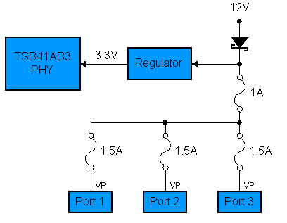
PHY and Port Power Supplies
The 1.5A reset-able fuses (Raychem SMD150) on the ports are designed to prevent excessive current if ports are accidentally shorted and the 1A fuse to protect the PMC +12V supply. Note that the PMCFW2 is not capable of providing external power from its ports other than the IEEE1394 requirement of 3W per port to power up other PHY'S on the IEEE1394 bus. The TSB41AB3 is configured to "advertise" itself during configuration as class 4 and alternate power provider.
LED Indicators
Six LED indicators are fitted, which can be viewed from the top of the board when it is fitted onto a host carrier. The functions are shown below.
LED Name |
Function | Colour |
CABLE |
Lit when cable attached | GREEN |
RECEIVE |
Lit when receiving | RED |
TRANSMIT |
Lit when transmitting | RED |
400 |
TX/RX @ 400Mbits/sec | YELLOW |
200 |
TX/RX @ 200Mbits/sec | YELLOW |
100 |
TX/RX @ 100Mbits/sec | YELLOW |
Connections
Front Panel Connector
The PMCFW2 provides 3 IEEE1394 ports through the front panel. The figure below shows the IEEE1394 connections viewed from the front panel, as per the IEEE1394-1995 specification.
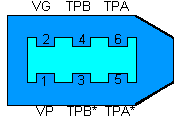
IEEE1394 Connections
IEEE1394 Connection Details
Cable assemblies consist of two plug connectors, either the 6-pin connector specified by IEEE standard 1394-1995 (with power) or the 4-pin connector defined by IEEE1394a (without power), joined by a length of cable. The PMCFW2 provides the 6-pin connector (with power), but can connect to a 6-pin or 4-pin IEEE1394 peripheral device.
The suggested maximum length of a cable assembly is 4.5m. This is to ensure that the maximum configuration of a set of cables does not exceed the length over which the end-to-end signal propagation delay would be exceeded. Longer cable lengths are possible if special consideration is given to the actual serial bus system topology to be used.
The figure below shows the 6-pin connector to 6-pin connector cable assembly, and below that the 6-pin connector to 4-pin connector cable assembly. The two signal pairs "cross" in the cable to effect a transmit-to-receive interconnection.
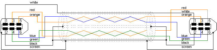
IEEE1394 6-pin to 6-pin Cable
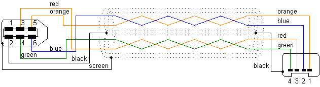
IEEE1394 6-pin to 4-pin Cable
PCI Connections
P1 and P2 provide the standard PCI signals on the PMC module, as defined in the PMC specification and reproduced for reference purposes below.
P1 32 Bit PCI |
P2 32 Bit PCI |
|||||||
Pin |
Signal Name |
Signal Name |
Pin |
Pin |
Signal Name |
Signal Name |
Pin |
|
1 |
TCK |
-12V |
2 |
1 |
+12V |
TRST# |
2 |
|
| 3 | Ground |
INTA# |
4 |
3 |
TMS |
TDO |
4 |
|
5 |
INTB# |
INTC# |
6 |
5 |
TDI |
Ground |
6 |
|
| 7 | BUSMODE1# | +5V | 8 | 7 | Ground | PCI-RSVD* | 8 | |
9 |
INTD# |
PCI-RSVD* |
10 |
9 |
PCI-RSVD* |
PCI-RSVD* |
10 |
|
11 |
Ground |
PCI-RSVD* |
12 |
11 |
BUSMODE2# |
+3.3V |
12 |
|
13 |
CLK |
Ground |
14 |
13 |
RST# |
BUSMODE3# |
14 |
|
15 |
Ground |
GNT# |
16 |
15 |
3.3V |
BUSMODE4# |
16 |
|
| 17 | REQ# | +5V | 18 | 17 | PME# | Ground | 18 | |
19 |
V (I/O) |
AD[31] |
20 |
19 |
AD[30] |
AD[29] |
20 |
|
21 |
AD[28] |
AD[27] |
22 |
21 |
Ground |
AD[26] |
22 |
|
23 |
AD[25] |
Ground |
24 |
23 |
AD[24] |
+3.3V |
24 |
|
25 |
Ground |
C/BE[3]# |
26 |
25 |
IDSEL |
AD[23] |
26 |
|
27 |
AD[22] |
AD[21] |
28 |
27 |
+3.3V |
AD[20] |
28 |
|
29 |
AD[19] |
+5V |
30 |
29 |
AD[18] |
Ground |
30 |
|
31 |
V (I/O) |
AD[17] |
32 |
31 |
AD[16] |
C/BE[2]# |
32 |
|
33 |
FRAME# |
Ground |
34 |
33 |
Ground |
PMC-RSVD |
34 |
|
35 |
Ground |
IRDY# |
36 |
35 |
TRDY# |
+3.3V |
36 |
|
37 |
DEVSEL# |
+5V |
38 |
37 |
Ground |
STOP# |
38 |
|
39 |
Ground |
LOCK# |
40 |
39 |
PERR# |
Ground |
40 |
|
41 |
SDONE# |
SBO# |
42 |
41 |
+3.3V |
SERR# |
42 |
|
43 |
PAR |
Ground |
44 |
43 |
C/BE[1]# |
Ground |
44 |
|
45 |
V (I/O) |
AD[15] |
46 |
45 |
AD[14] |
AD[13] |
46 |
|
47 |
AD[12] |
AD[11] |
48 |
47 |
Ground |
AD[10] |
48 |
|
49 |
AD[09] |
+5V |
50 |
49 |
AD[08] |
+3.3V |
50 |
|
51 |
Ground |
C/BE[0]# |
52 |
51 |
AD[07] |
PMC-RSVD |
52 |
|
53 |
AD[06] |
AD[05] |
54 |
53 |
+3.3V |
PMC-RSVD |
54 |
|
55 |
AD[04] |
Ground |
56 |
55 |
PMC-RSVD |
Ground |
56 |
|
57 |
V (I/O) |
AD[03] |
58 |
57 |
PMC-RSVD |
PMC-RSVD |
58 |
|
59 |
AD[02] |
AD[01] |
60 |
59 |
Ground |
PMC-RSVD |
60 |
|
61 |
AD[00] |
+5V |
62 |
61 |
ACK64# |
+3.3V |
62 |
|
63 |
Ground |
REQ64# |
64 |
63 |
Ground |
PMC-RSVD |
64 |
|
Programming
Windows® Software
The PMCFW2 is both an Open Host Controller Interface 1.0 (OHCI) and IEEE1394a compliant Link-layer device (LYNX), and support for this is built in to Windows®98SE, Windows®ME and Windows®2000. Additional software may be supplied by peripheral vendors. As the module is OHCI compliant various other packages are available from third party vendors providing support for VxWork, LynxOS etc.
Specification
On-Board Functions
TSB12LV26 IEEE1394 Controller
Texas Instruments TSB12LV26 PCI-to-IEEE1394 Host Controller.
PCI Local Bus Revision 2.2.
PCI Bus Power Management Interface Revision 1.1.
IEEE 1394-1995, 1394a, and 1394 Open Host Controller Interface.
IEEE1394 link data rates of 100 Mbits/sec, 200 Mbits/sec, and 400 Mbits/sec.
PC99 compatible.
TSB41AB3 IEEE1394a-2000 PHY
Texas Instruments TSB41AB3 IEEE1394a-2000 3-Port Cable Transceiver/Arbiter.
2 differential line transceivers per port.
Connection status monitoring, initialisation, and arbitration functions.
Packet reception and transmission.
Board Configuration
EEPROM: 2Kbits - PCI & IEEE1394 Configuration
LED Indicators (6): CABLE, RECEIVE, TRANSMIT, 400, 200, 100
PMC Interface
Bus Interface: PCI 2.2 compliant
Bus Width: 32-bit
Data Transfer: PCI 2.2 Bus Mastering
Interrupts: PCI INT #A
Memory Address: BIOS assigned
PCI configuration: DWORD, WORD & BYTE
Operating Environment
Dimensions: 74.0mm x 149.0mm (single PMC size)
Power: +3.3V TBDmA typical, +12V TBDmA typical when idle
+3.3V TBDmA typical, +12V TBDmA typical when connected
Environmental: 0 to 70 ° C, 95% humidity non-condensing (extended range to order)
BVM Limited can be contacted by Telephone +44 (0)1489 780144 Fax
+44 (0)1489 783589
|